OH2NLT Experimental Digital HF transmitter-II
28.01.2008
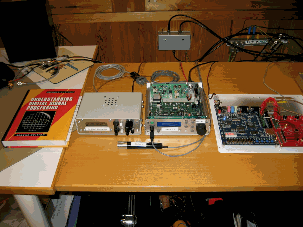
OH2NLT Digital_TX-II at the middle.
Original
Digital_TX prototype on the right side and Digital receiver on the left side.There are plenty of PC based digital radio projects around. Personally I like to experiment with stand-alone equipment. Good results with the first prototype and success with VHDL learning inspired me to design my own Digital TX board. There are no ready integrated circuits for transmitter chain like AFEDRI8201 for the receiver. I decided to make a "evolution version" of my first prototype done with Altera Cyclone-II FPGA. Selecting the FPGA chip was little bit challenging. Most of the large FPGA chips are available only in high pin count BGA versions. What I needed was large number of logic elements but not plenty of I/O pins. TQFP package is also easier t solder than BGA with homebrewer tools. Altera Cyclone-III series offered suitable part. EP3C25 in 144 EQFP package. There are some tricks with the EQFP package. More about EQFP package later. With Matti OH7SV we have designed
JUMA-TRX2 transceiver. I decided to use JUMA-TRX2 enclosure and some of its modules. 10W PA board can be used as is. TRX2 DDS board without DDS chip is good platform to implement Digital TX user interface.With different versions of VHDL code board can be configured:
Digital TX schematic diagram
Page1 RF DAC & RF amplifier | Page2 Power supply & JTAG
Page3 Connectors &control interface | Page4 Audio codec & Ref oscillator
Control board schematic diagram.
Control board is partially populated JUMA-TRX2 DDS board. DDS chip is not needed in this application.
Page1 Power supply | Page2 Micro controller
PA board and connector board
Documentation can be found from
JUMA-TRX2 technical www pageDigital TX board VHDL code is early version of code containing all sort of tests end experiments.
Digital TX PCB lay out is not particularly dense. Design is done on two-sided PCB. Main goal have been to keep ground copper plane as whole as possible. There is also room for future experimentation like another RF output if DAC5672 is used. For single RF output also DAC2904 can be used. First revision of VHDL code uses 50MHz oscillator, which is directly used as RF sample rate. There is place for another oscillator and of course FPGA PLLs can be used for reference frequency generation. Special arrangement is ended to solder the EP3C25E144 Cyclone-III EQFP chip. There is a GND pad in the middle of the bottom side of the chip what must be electrically connected to ground. I made special decal for this chip. There is a 3mm-plated hole in the PCB through what GND pad soldering can be done. Digital TX board needs several operating voltages. Linear regulators are used despite of poor efficiency to keep RFI down. Cyclone-III in 65nm chip and core voltage is only 1.2V. Maximum I/O voltage is 3.3V. There is Altera application note AN447 available explaining low voltage I/O design requirements. This low voltage issue concerns also JTAG interface and boot flash interface.
Some links